The benefits of PCB testing
Many electronic products present faults in the prototyping phase that designers have to solve before they reach the market in order to avoid serious problems.
Testing electronic products, namely PCBs during their assembly, prevents these problems from occurring and is vital to meet requirements and quality standards.
There are a variety of test methods that can be performed on prototypes or small-scale units, allowing identification of problems in the design or layout with the following benefits:


PCB testing methods
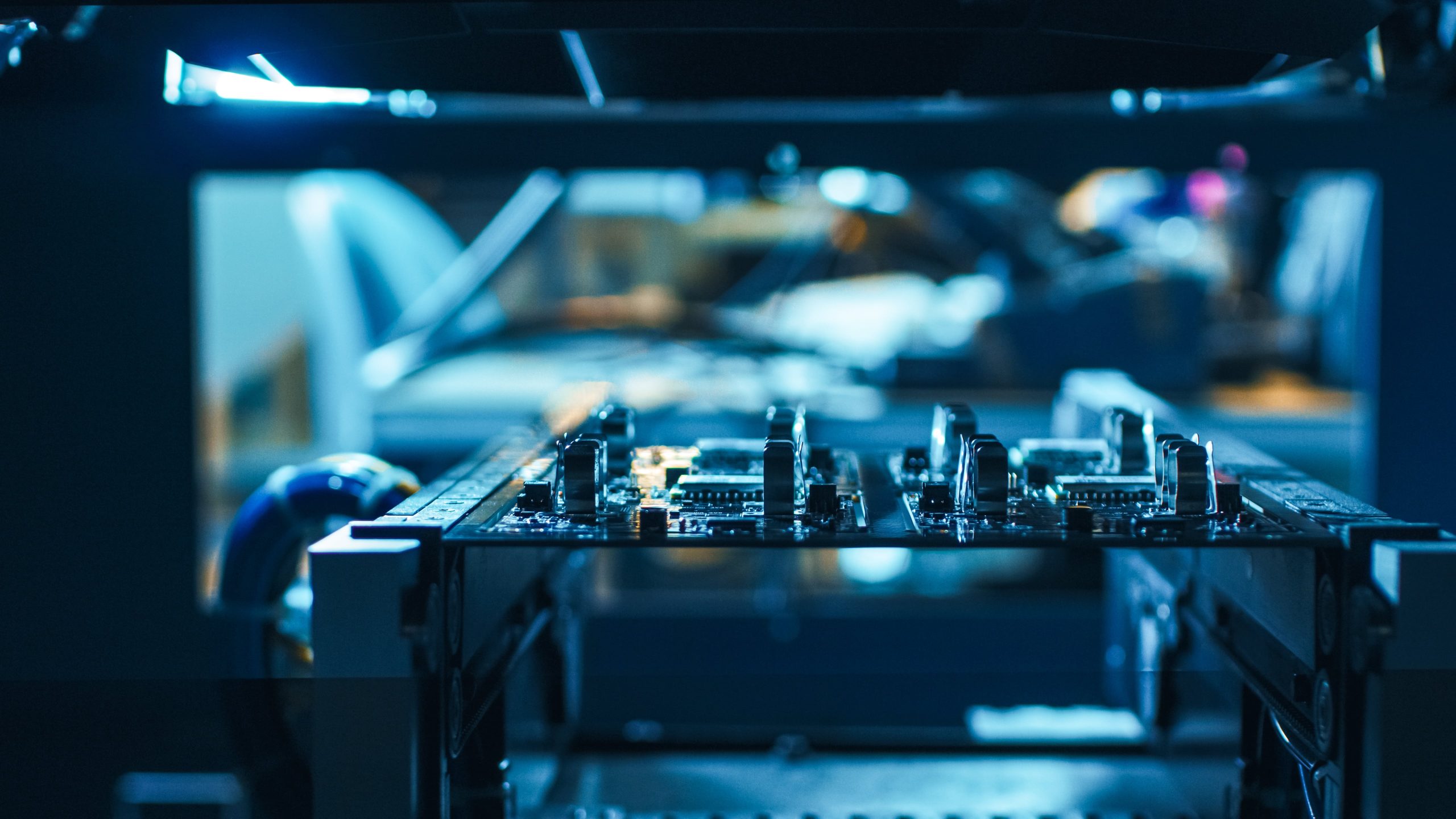
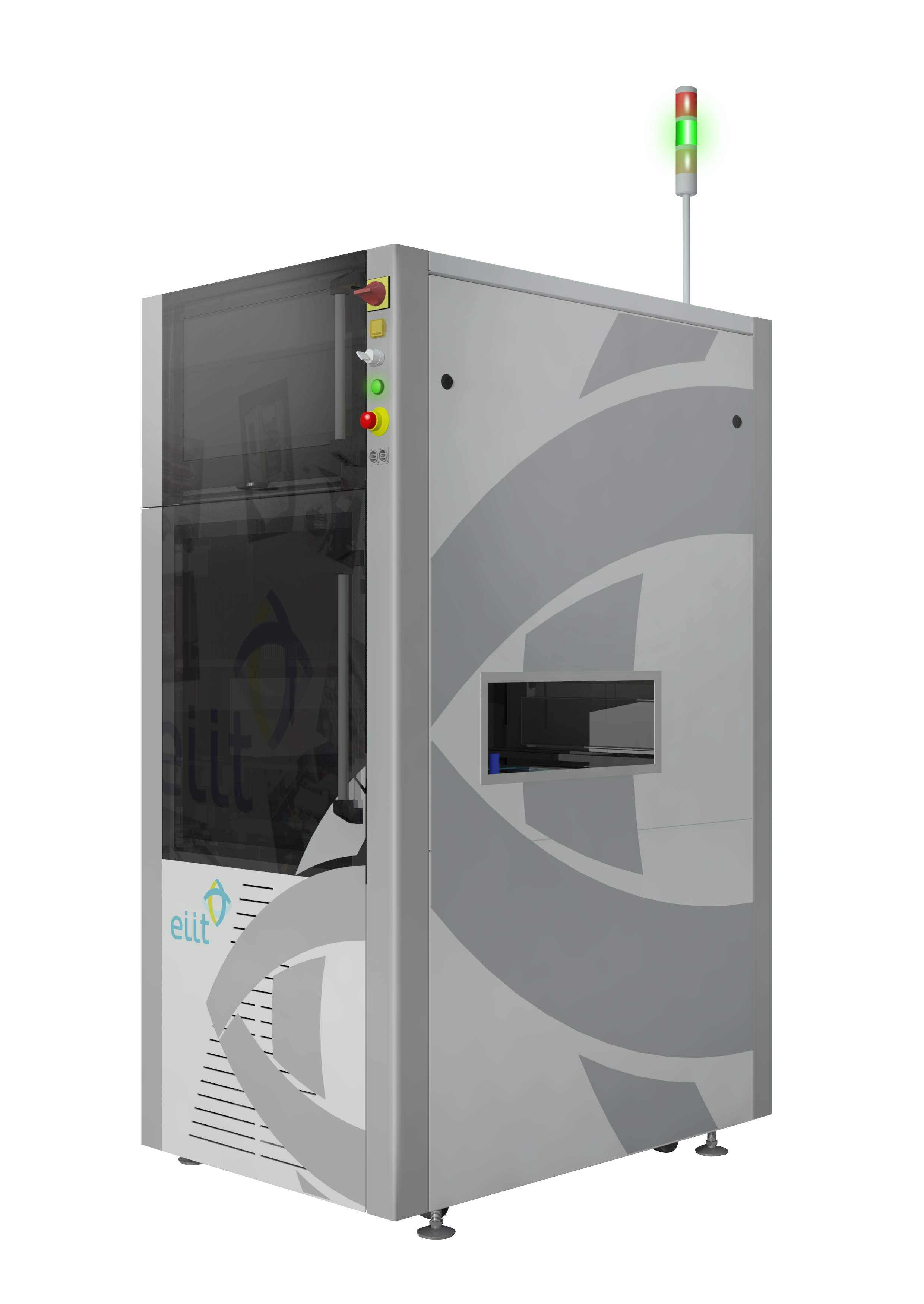
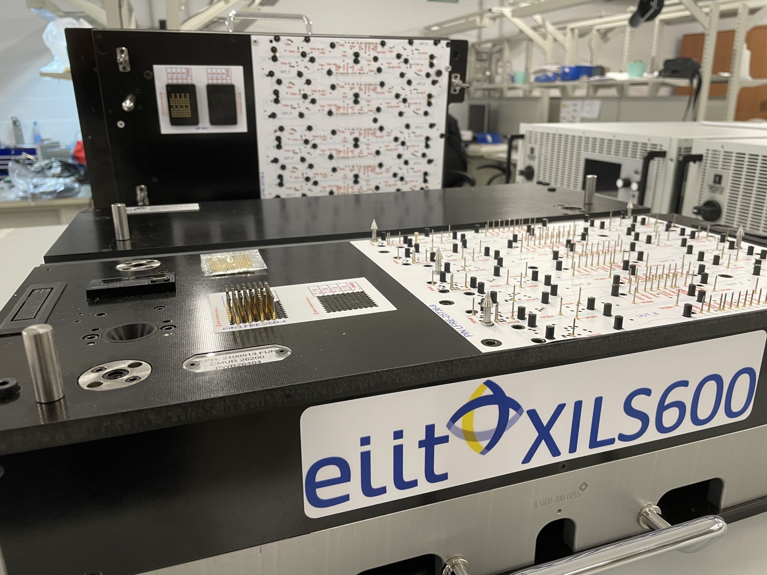
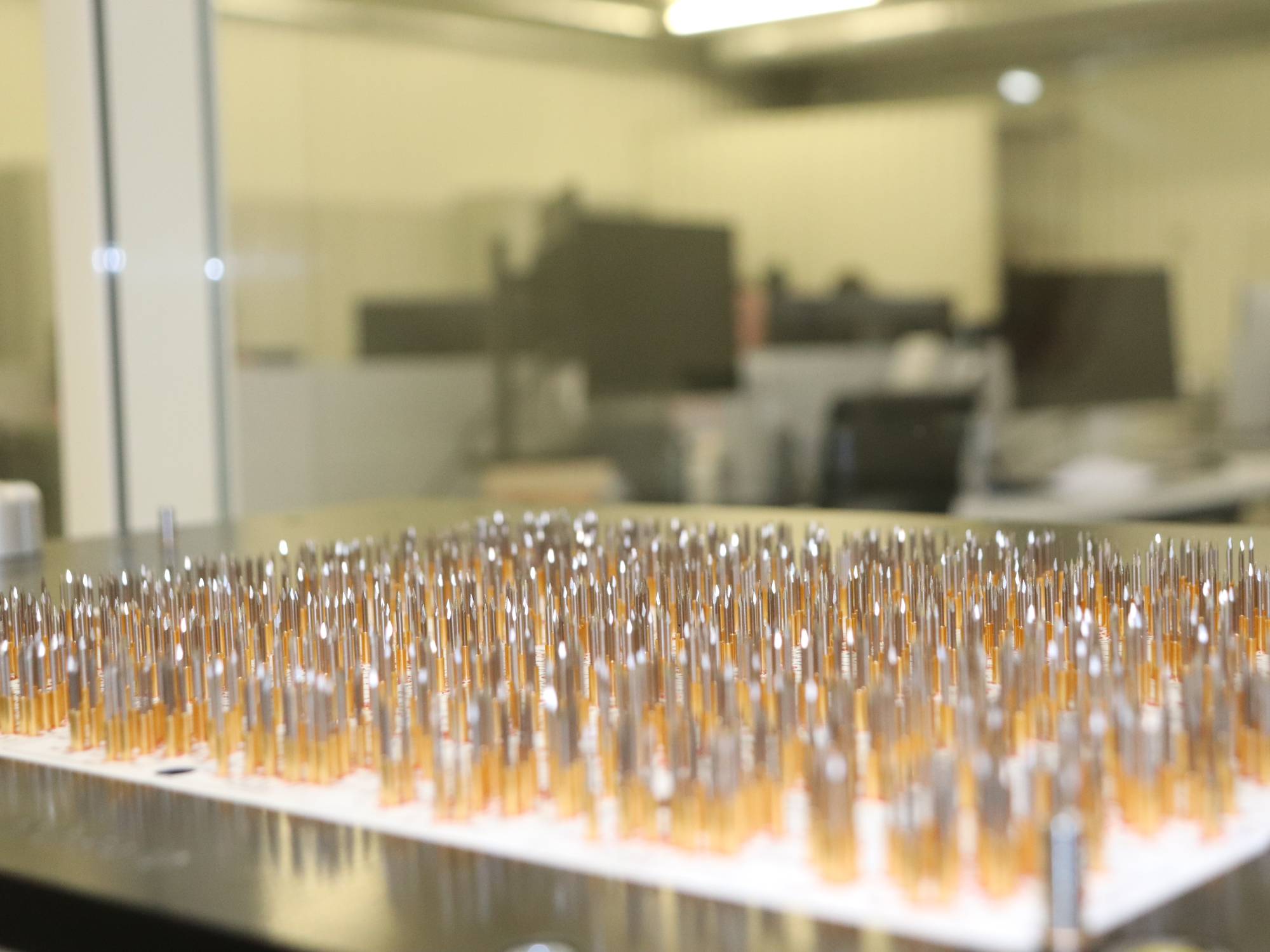
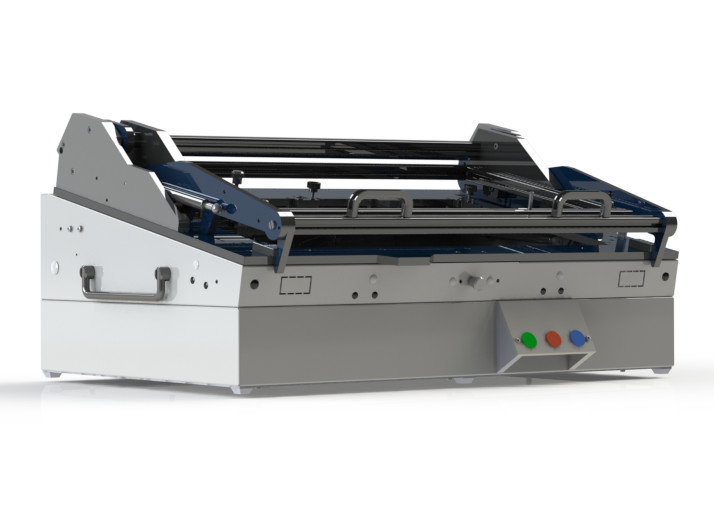
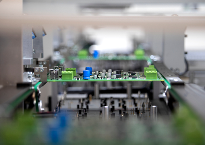
In-Circuit Testing (ICT): this involves testing the individual components on the PCB while they are connected to the circuit board. It is performed after the assembly stage to verify the correct functioning and position of each electronic component on the PCB. For this purpose, a flying probe composed of an array of drivers and sensors is used to perform the measurements required by the test by moving freely on the board.
Such method requires:
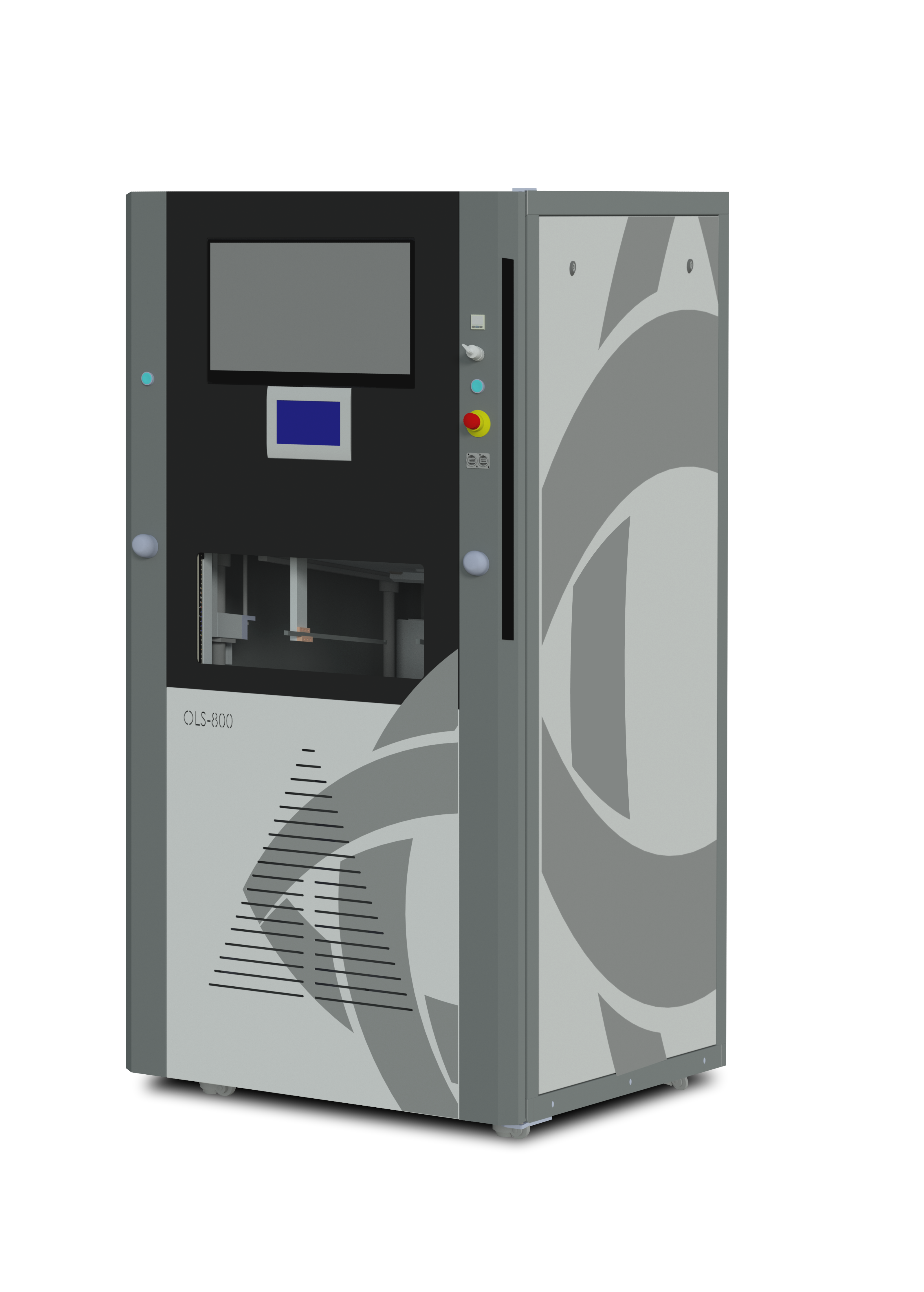
- In-circuit tester: performs measurements for the test through a range of sensors and drivers. Controlar and EIIT – a Controlar company have available automated inline systems (in a serial layout) or cost-effective easy-to-install offline models.
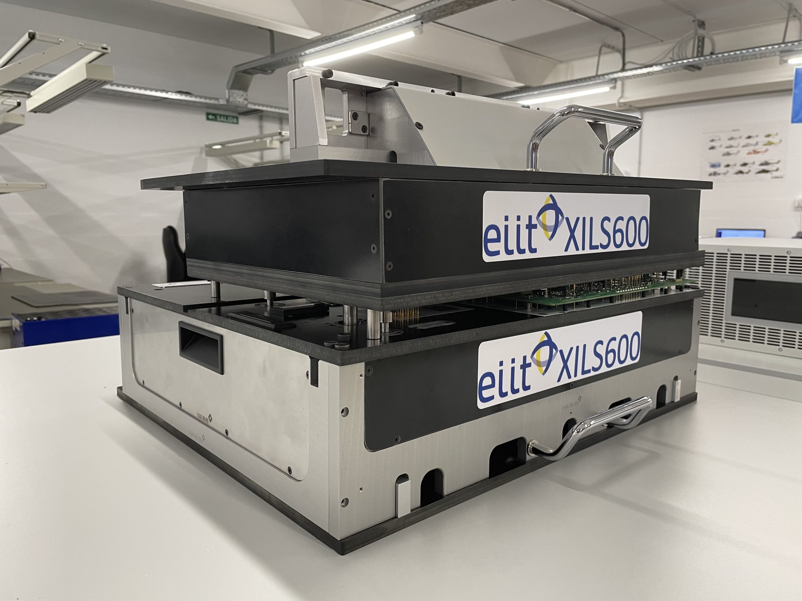
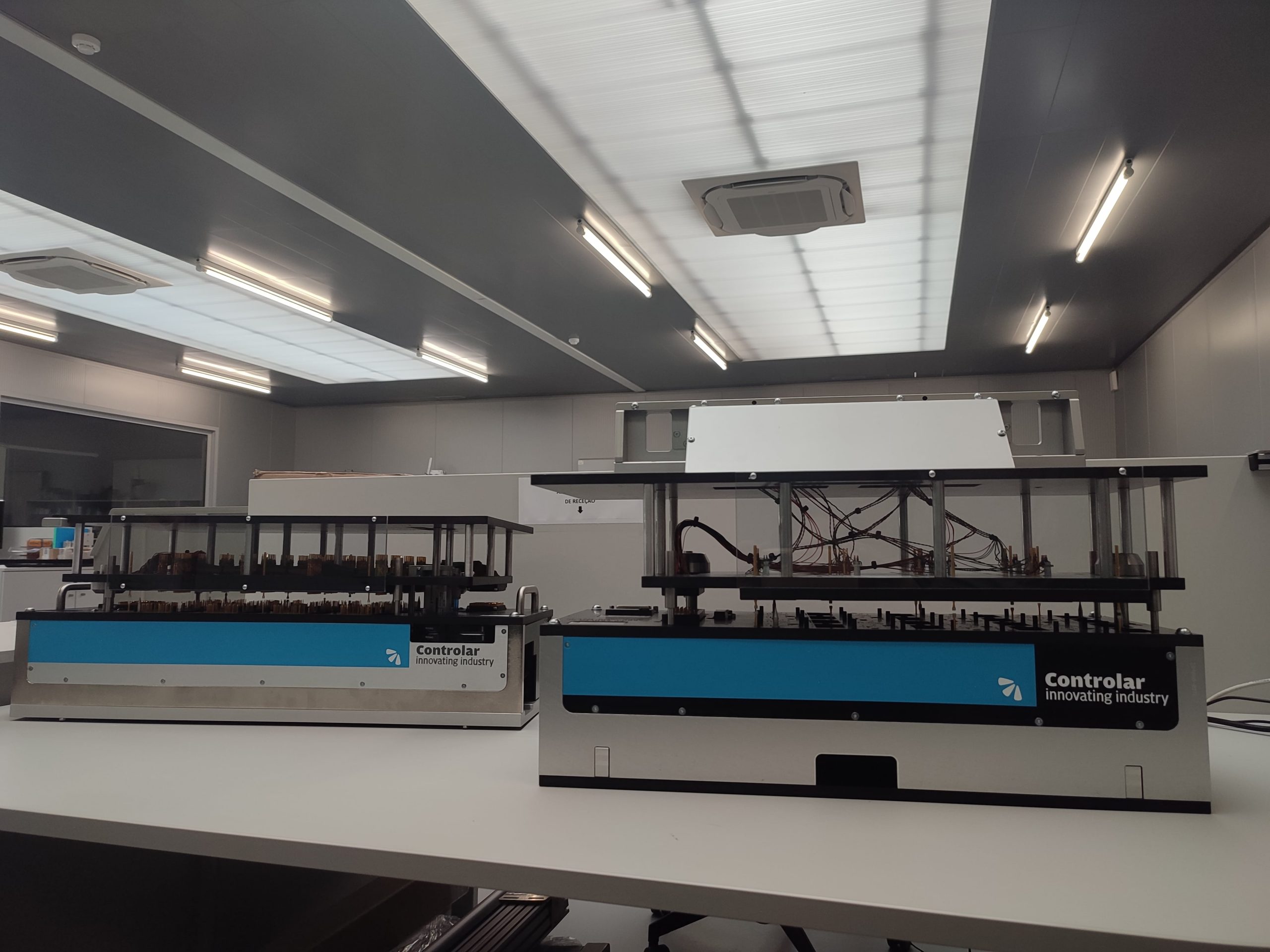
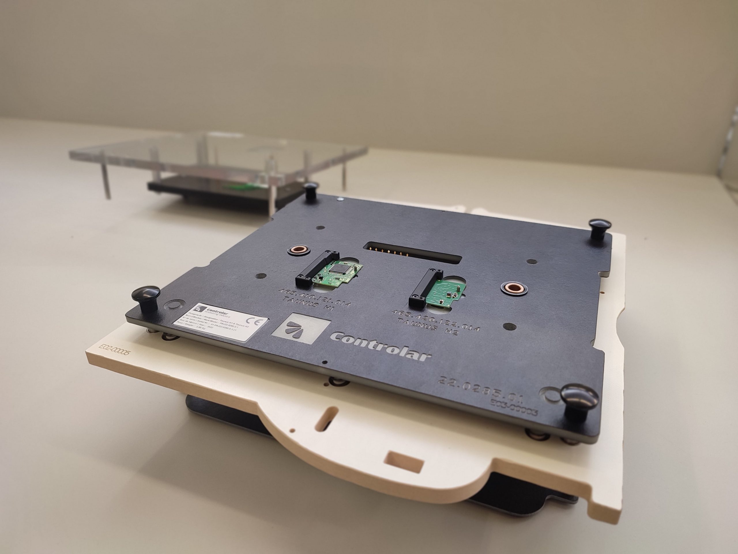
- Fixture: integrated into the tester, interacts directly with the board to be tested. Much like a bed of nails, the fixtures are the most expensive part of the system. Our companies develop and supply tooling and test fixtures for all kind of applications.
- Software that dictates the type of test for each type of PCB and the parameters for passing or failing. All our software is developed inhouse.
ICT is quite popular among manufacturers, capable of finding 98% of failures.
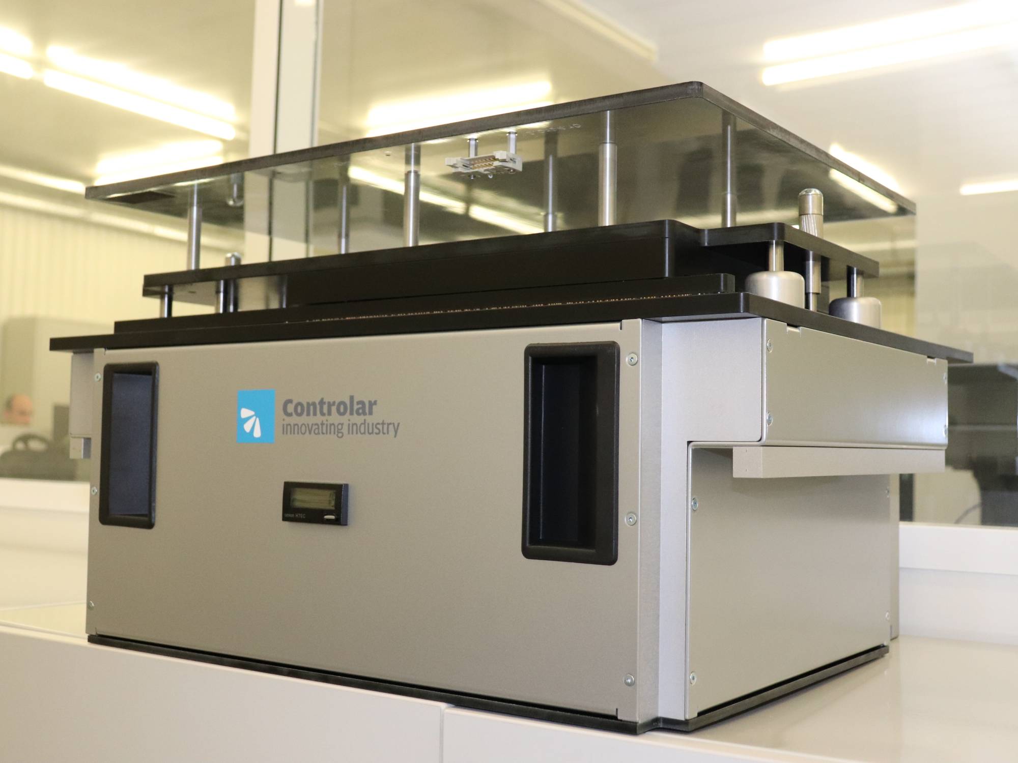
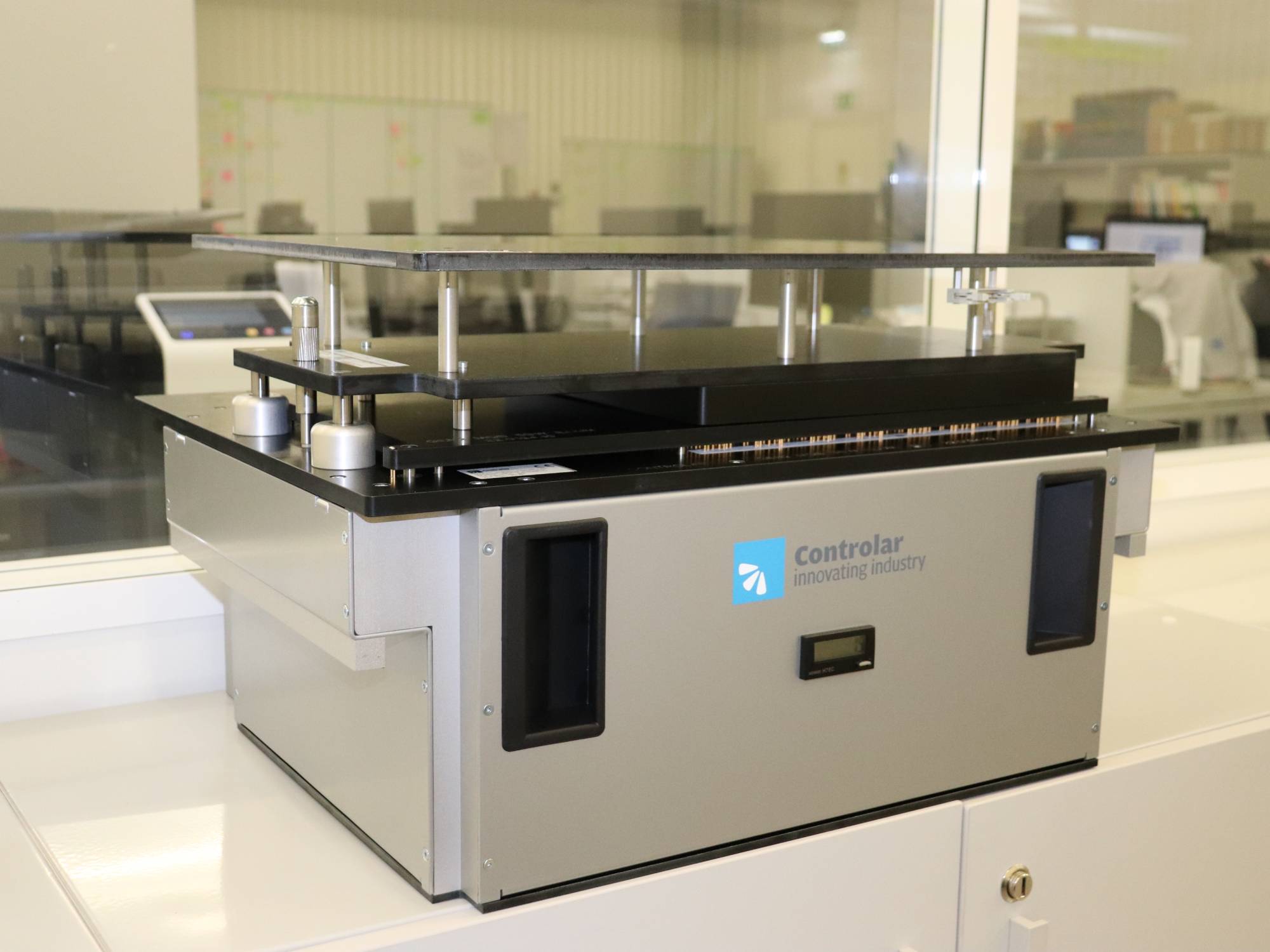
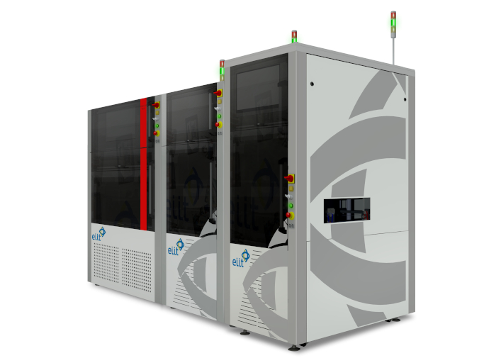
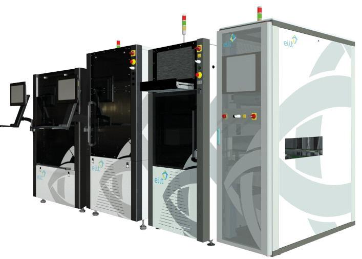
Being the last step of the inspection and verification process, functional test is typically performed at the end-of-line, using a functional test system to validate whether the PCBs meet the specifications or not.
As the name implies, this method tests the functioning of a circuit, by applying power and testing its performance against specific requirements. It aims at reproducing the electrical signals and measuring the effects produced, i.e., simulating the final environment in which the PCB is supposed to work in.
The main advantage of the functional test is its possibility to detect potential circuit anomalies that occur only when the circuit is powered. The disadvantages are related to the cost and complexity of the test system. Most available equipment is not very flexible and is configured to perform only the test of a specific card.
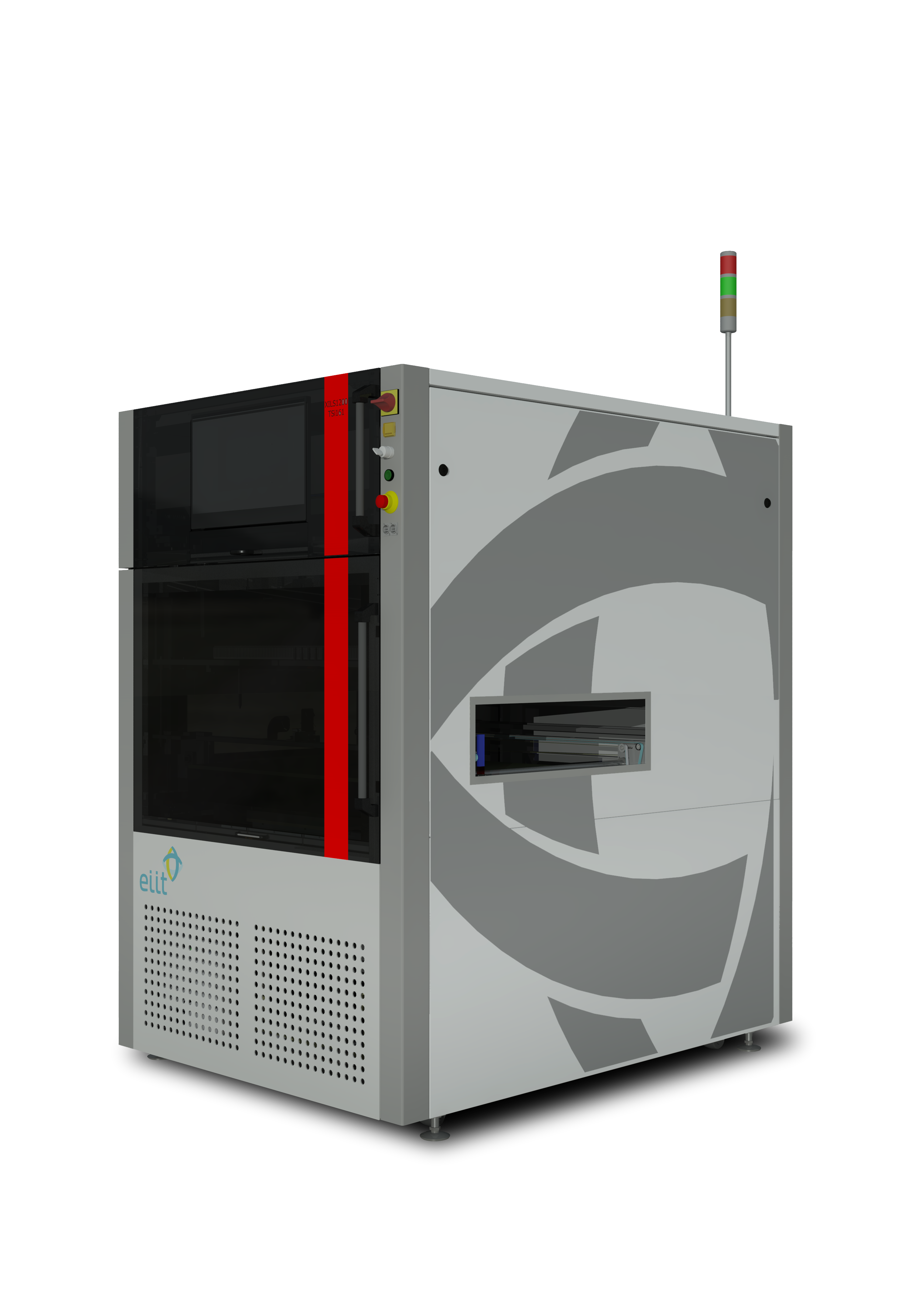
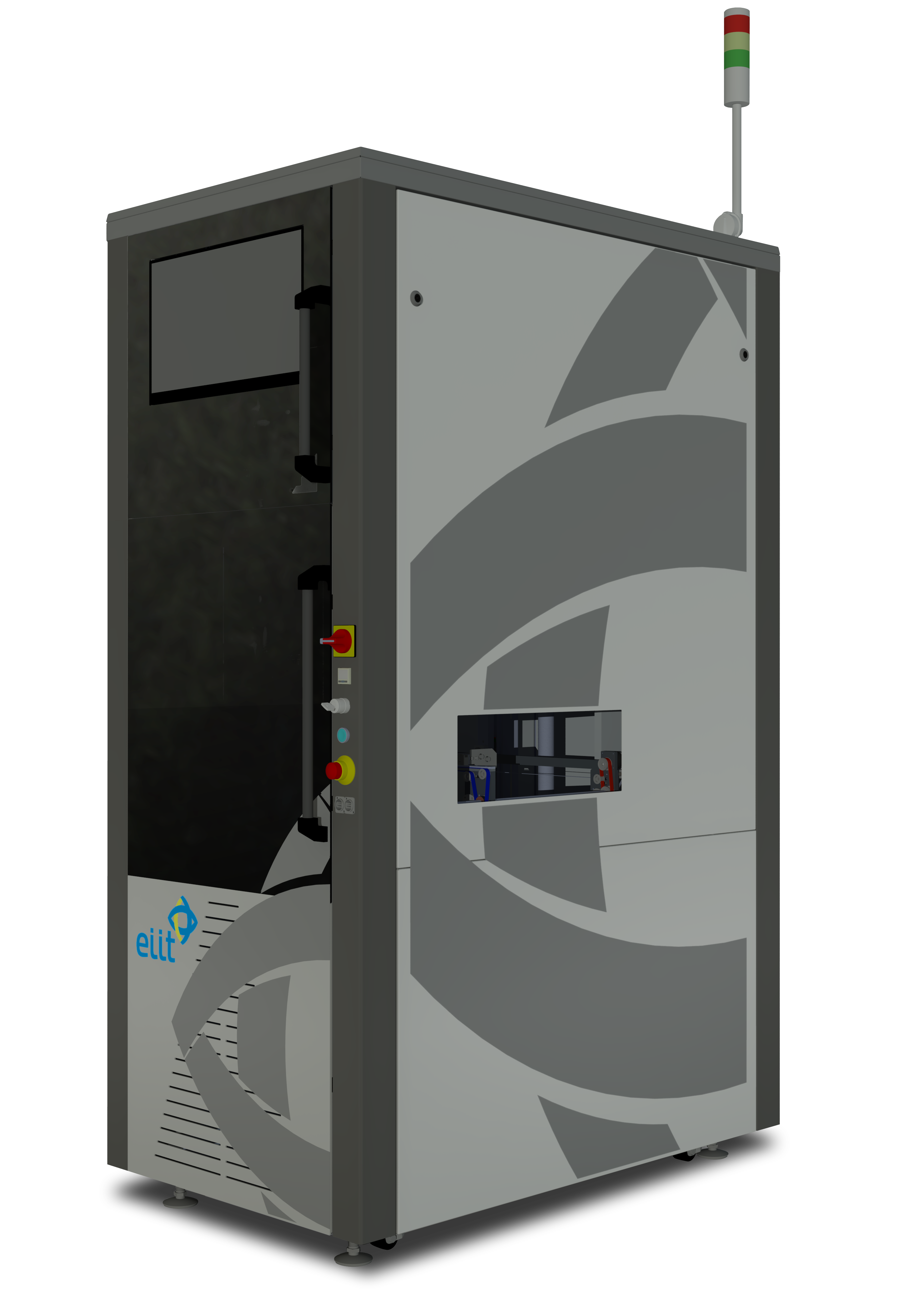
Controlar and EIIT – a Controlar company have over 25 years of experience in developing functional test systems and now integrate solutions in their portfolio that work around this challenge.
As an example, Controlar has developed TSIM – Test System Intelligent Machine, a highly flexible and modular test solution, that allows the performance of a different level of functional tests on a wide range of devices and downsizes the fixtures replacement time.
Commonly used to test the interconnections between the components on the board when it is not possible to reach the nodes of the circuit, this method is quite versatile and can be used to detect problems in functioning systems directly on the field.
The boundary scan method has the advantage of being suitable for several applications, including system-level test, RAM and flash memory test, flash programming and CPU (Central Processing Unit) emulation, among others.
Our ISP Consoles are the ideal option to address some of these challenges, such as programming of flash memories.
Many of these methods have a high cost due to their complexity and technology involved, which are not always suitable for simpler products. Our departments develop jigs and manual test consoles, more suitable for these particular cases.
Regardless of which method is chosen, PCB testing represents a fundamental step in the electronic design process by identifying possible defects affecting the circuit before it reaches final production, ultimately saving a lot of time and money.
Get in touch with Controlar or EIIT to find out more or download our brochures:


