PicAI
AI Precision for ICT Fixtures
The Challenge
Accuracy vs. Reliability
In the production of printed circuit boards (PCBs), In-Circuit Testing (ICT) is one of the most widely used methods to ensure electrical functionality. This testing relies on fixtures known as “beds of nails,” where hundreds or even thousands of spring-loaded probes must make precise mechanical contact with the designated test points on the PCB.
Even small misalignments can have serious consequences. If a probe misses the intended test point, measurements may not reflect the true condition of the circuit, leading to false positives (defective boards incorrectly validated) or false negatives (good boards rejected). Both outcomes are costly: the former risks product failures downstream, while the latter introduces unnecessary rework and waste. Repeated misalignment can also damage pads and shorten PCB lifespan.
To mitigate these risks, manufacturers conduct conformity checks on ICT fixtures. However, in most facilities this process is still highly manual: operators inspect probe alignment under microscopes, often checking only a sample of test points. With hundreds of pads per PCB, this approach is slow, labor-intensive, and prone to variability, allowing minor misalignments to escape detection.
As PCB complexity increases and production volumes grow, ensuring a reliable, efficient, and scalable method for probe alignment verification has become a critical requirement in modern electronics manufacturing.
The Technology
Automation, AI, and Precision Mechanics
The key to reliable ICT lies in accurate probe-to-test-point alignment. Automated approaches replace subjective manual inspection with computer vision, artificial intelligence (AI), and precision mechanics, achieving micrometer-level accuracy.
High-resolution imaging captures each pad, often less than 1 mm in diameter, and detects punctures as small as 25 µm. AI algorithms then analyze these images, distinguishing acceptable contact marks from problematic misalignments, while calculating exact deviations from the pad’s center.
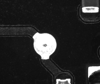
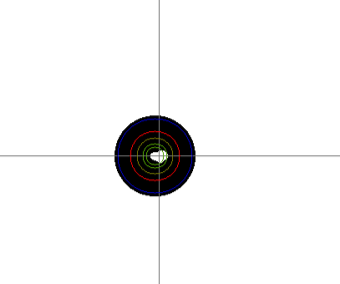
Comparison of raw vision system capture (left) and AI-processed analysis (right), showing probe marks, test point centers, and deviations. Slide to explore.
Achieving this requires:
-
Precision mechanics – motion stages and handling systems that position the PCB and vision sensors with micrometer repeatability.
- Robust structural design – minor vibrations or misalignments in the mechanical system can lead to measurement errors at this scale.
-
Optimized optics – premium lenses, high-speed cameras, and multi-angle or structured lighting designed to minimize distortion and highlight subtle punctures while avoiding shadows and reflections.
-
AI-driven analysis – trained models that adapt to different PCB materials, colors, pad geometries and surface finishes, ensuring consistent detection across diverse designs. Advanced image analysis algorithms can filter out noise, compensate for minor illumination inconsistencies, and identify defects that would be difficult or impossible to detect manually.
This combination of AI-driven analysis with precision optics and mechanics ensures full coverage, repeatable results, and a robust assessment of probe alignment that scales with production volume.
The Benefits in Practice
By automating probe alignment and puncture detection, manufacturers gain clear advantages:
The Application in Electronics Manufacturing
Automated inspection is particularly valuable in high-volume, high-complexity environments. Every test point can be verified with micrometer precision, ensuring ICT fixtures are properly aligned and test results reflect the true electrical condition of the boards.
This not only improves product reliability but also reduces costly rework and accelerates production cycles. When fixtures are customized for each PCB variant, automated systems minimize alignment errors and provide the repeatability required to scale operations efficiently.
The Solution
PicAI - AI-Driven Probe Inspection Control System
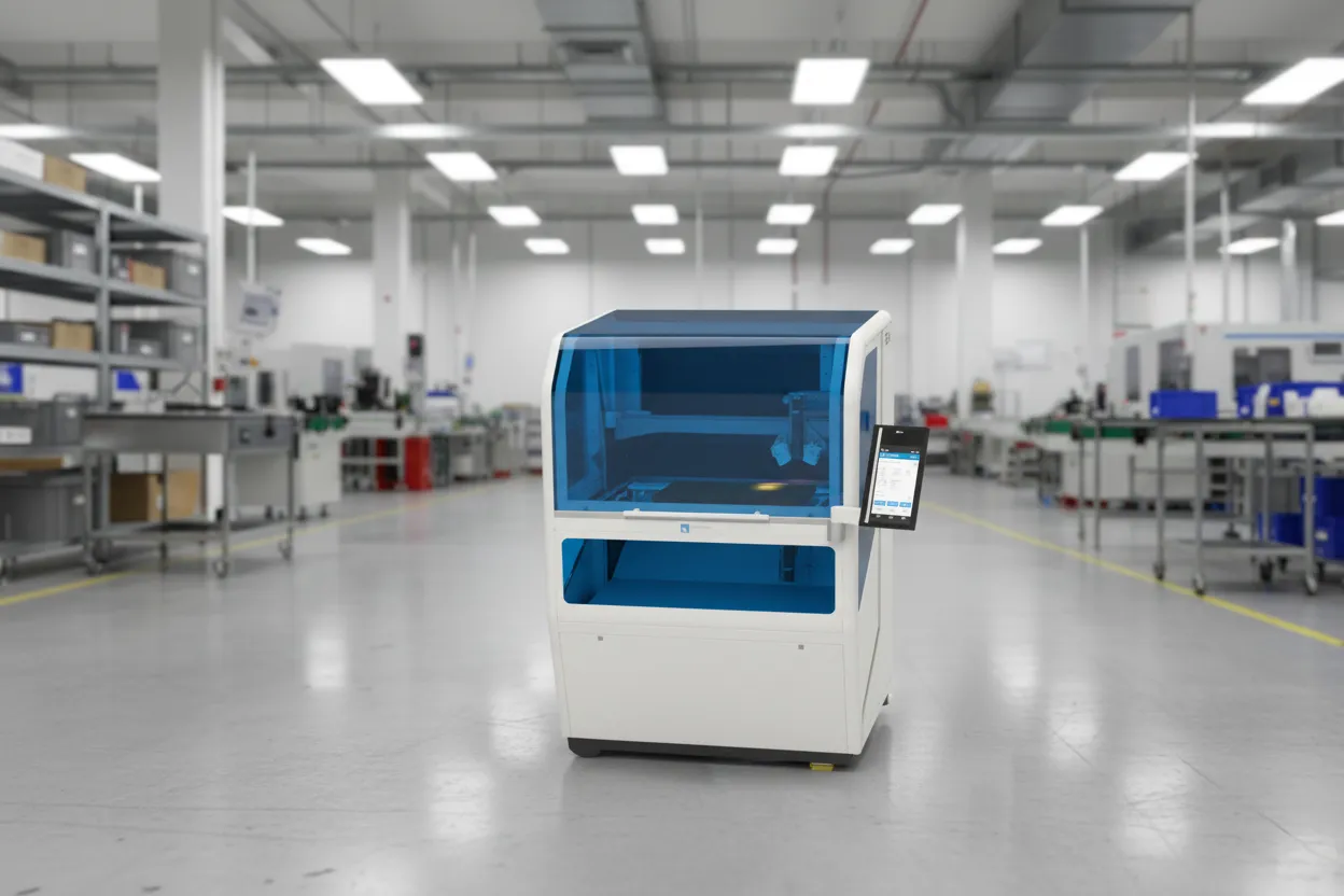
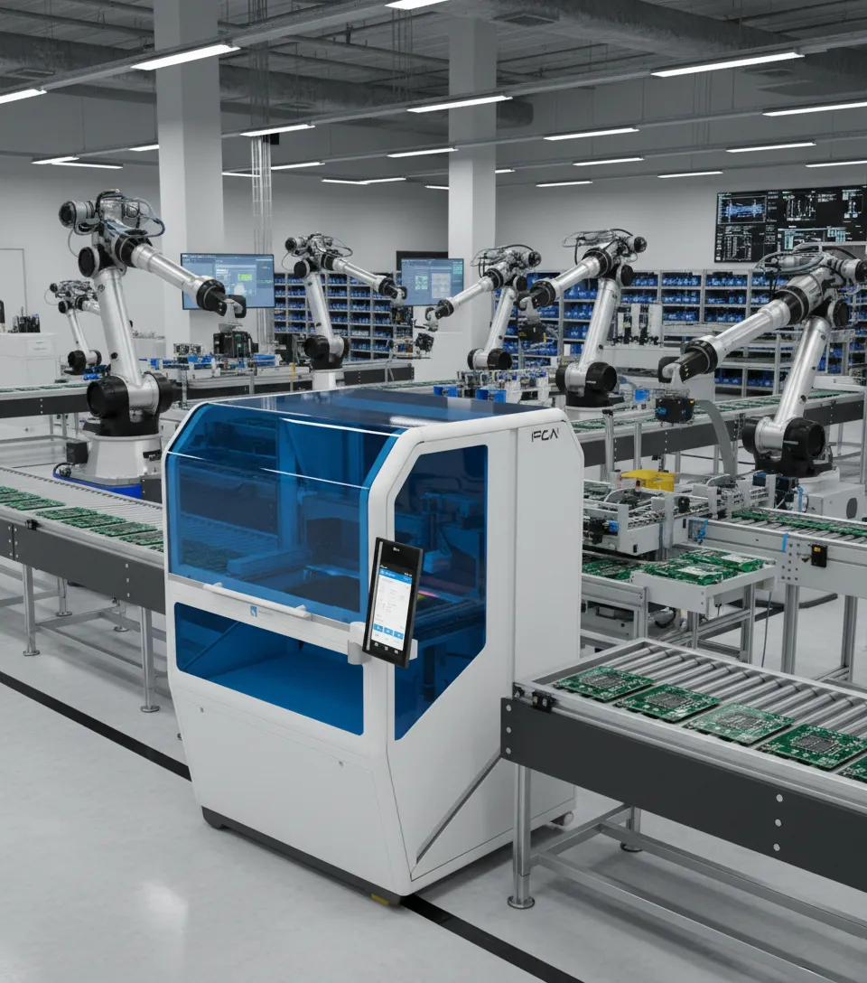
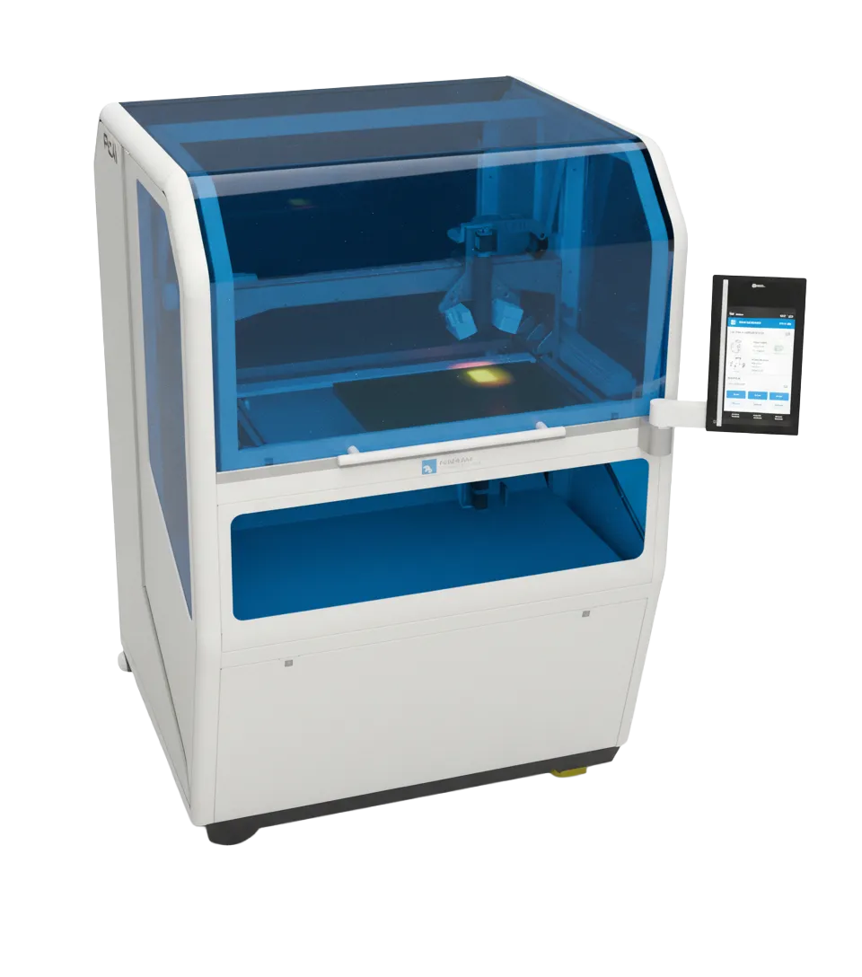
These principles of precision, automation, and AI-driven inspection are realized in PicAI – AI-Driven Probe Inspection Control system, a patent-pending solution designed for high-accuracy verification of PCB probe alignment.
PicAI can inspect boards up to 500 × 500 mm, accommodating a wide range of PCB sizes, materials, and colors while maintaining a resolution of 7 μm, sufficient to detect even the smallest punctures. Two linear camera arrays capture the top and bottom sides simultaneously, scanning an entire PCB in just a few minutes, providing a rapid and scalable solution suitable for high-volume production environments.
Key features include:
-
Dual-side inspection for faster full-board coverage.
-
Micrometer-level precision mechanics for accurate positioning of the board relative to the cameras.
-
Optimized optical architecture with high-resolution lenses and controlled lighting guarantees consistent imaging across various PCB surface types.
-
AI-driven analysis capable of detecting punctures, misalignments, and calculate exact deviations.
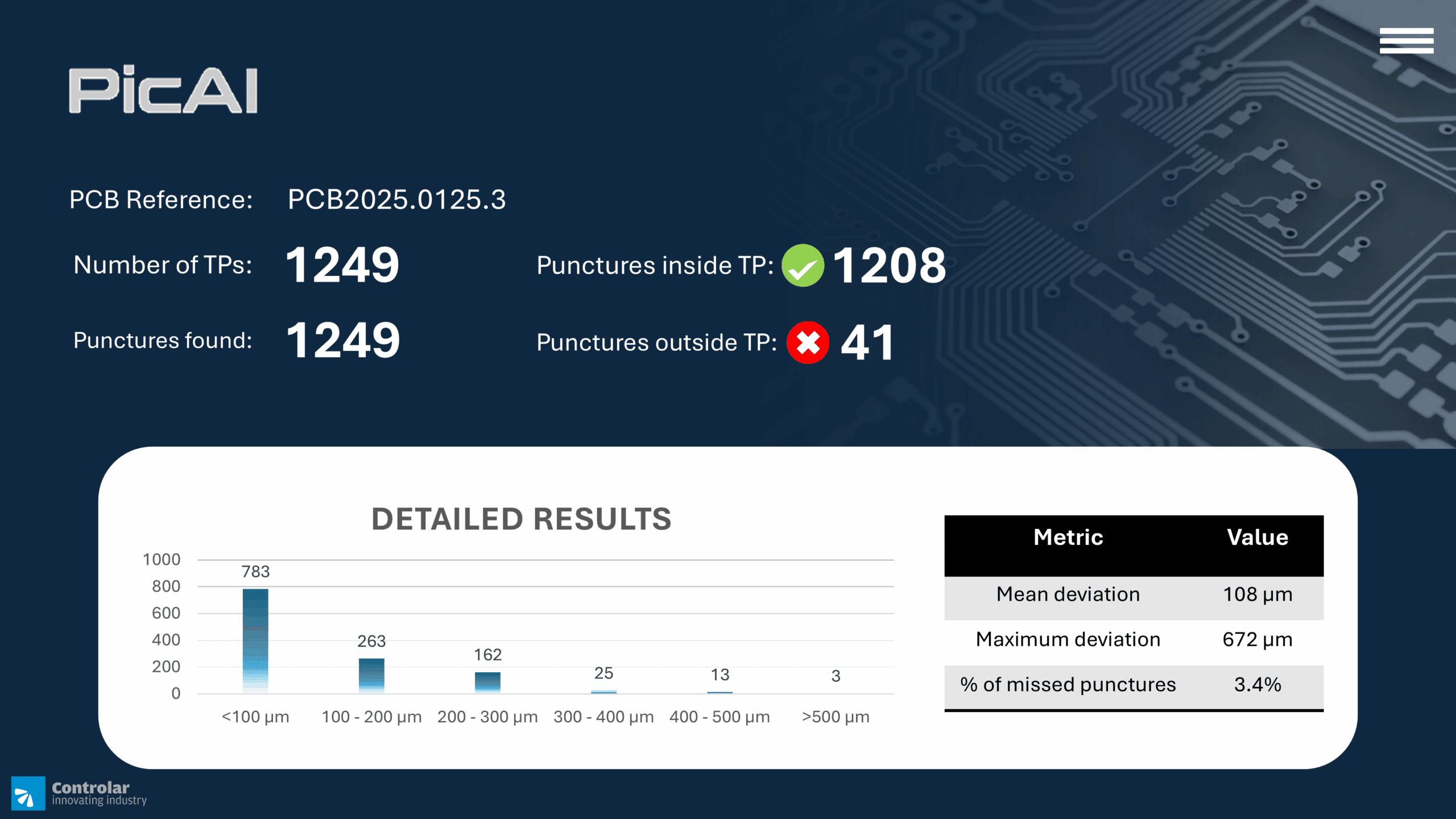
- Detailed reporting include both per-test-point alignment data and statistical measures across the entire PCB, allowing manufacturers to assess overall fixture performance and process consistency.
By combining high-resolution imaging, dual-sided inspection, precision mechanics, and AI algorithms, PicAI delivers a robust, efficient, and scalable solution for probe alignment verification, helping prevent production defects before they propagate downstream.
See PicAI live at productronica 2025 and discover how AI-driven inspection is setting new standards in ICT fixture validation.