Introduction
In the electronics industry, where system complexity is growing exponentially, the need for efficient methodologies for programming and testing devices is more critical than ever. Two fundamental technologies in this field are Flash Programming and Boundary Scan (JTAG), used in both the development and production of electronic systems.
This article delves into the technical principles, tools, standards, and best practices of these technologies, addressing their applications and impact on the industry.
Flash Programming: Architectures and Methods
Flash Programming is the process of writing data to non-volatile memory, essential for the operation of microcontrollers, EEPROM, NAND and NOR flash memories, FPGAs, and other programmable electronic devices. In industries where programming reliability and speed are critical, such as automotive and aerospace, this technology enables efficient loading and updating of firmware and embedded software.
Flash memory programming is a key phase in the manufacturing process of electronic boards, as it defines the system’s behavior and its ability to operate correctly in its final environment. Unlike other storage methods, flash memory offers low read latency, high endurance for write cycles, and durability in harsh environments, making it the preferred choice for embedded systems and control modules.
Given the high production volumes and complexity of modern devices, programming strategies must be optimized to ensure minimal cycle times without compromising product quality. In this context, our companies develop test solutions that integrate Flash Programming into its test benches, ensuring a fast and secure manufacturing process.
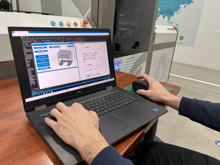
Flash Programming on XILS800-MY23 from EIIT – a Controlar company
Flash Memory Architectures
There are two main flash memory architectures:
- NOR Flash
- Fast random access, ideal for executing code directly (Execute-In-Place, XIP).
- Used in embedded microcontrollers and real-time critical systems.
- Slower programming and lower storage density compared to NAND.
- NAND Flash
- Higher storage density and lower cost per bit.
- Used in mass storage applications (eMMC, SSDs, USB drives, SD cards).
- Requires advanced error correction techniques (ECC, Error Correction Code).
Flash Programming Methods
In-System Programming (ISP)
- Allows programming the flash memory within the system without removing the chip.
- Performed via interfaces such as JTAG, SWD (Serial Wire Debug), or SPI.
- Useful for firmware updates in finished devices.
In-Circuit Programming (ICP)
- Similar to ISP but accessed through specific PCB pins.
- Requires dedicated hardware programmers.
Pre-Programming (Off-Board Programming)
- Flash memory is programmed before assembly in the production line.
- Faster for mass production but less flexible for later updates.
Protocols Used in Flash Programming
- JTAG (IEEE 1149.1): Used for both programming and diagnostics.
- SWD (Serial Wire Debug, ARM Cortex-M): Lower pin count alternative to JTAG.
- I2C / SPI: Common interfaces for serial memories in embedded systems.
- UART Bootloaders: Used for firmware updates in many microcontrollers.
Challenges in Flash Programming
- Programming time: As firmware sizes increase, write speed becomes a critical factor in production.
- Data corruption protection: Implementation of ECC and redundancy in NAND Flash.
- Code security and protection: Use of techniques such as Secure Boot and firmware encryption to prevent tampering.
Boundary Scan (JTAG): Contactless PCB Testing
Boundary Scan is a technique based on the IEEE 1149.1 standard that enables the testing of interconnections on printed circuit boards (PCBs) without the need for physical probes or direct access to components. This technology is crucial for detecting manufacturing defects, debugging, and validating embedded hardware.
Boundary Scan Structure and Functionality
Each JTAG-compatible device includes a chain of shift registers (Scan Chain) connected to the chip’s input and output pins. These registers allow:
- Forcing specific states on input/output (I/O) pins.
- Reading internal device states without interrupting its operation.
- Performing structural and functional tests without direct physical access.
Key Components in Boundary Scan
- Tap Controller: Controls the scan sequence through a set of predefined states (Test-Logic-Reset, Shift-IR, Shift-DR, etc.).
- Instruction Register (IR): Defines the commands executed on the device.
- Data Registers (DR): Contain relevant test information.
- Test Access Port (TAP, con pines TDI, TDO, TCK, TMS): Physical access point to the device.
Advanced Applications of Boundary Scan
PCB Integrity Verification
- Identification of short circuits, disconnected pins, and soldering defects.
- Validation of assembly in mass production.
Digital Component Testing
- Diagnosing failures in FPGAs, microcontrollers, and ASICs without in-situ debugging.
Firmware and FPGA Bitstream Programming
- Flash Programming via JTAG in memories connected to SoCs or microcontrollers.
Test Tools
- JTAG Boundary Scan Testers (BSTs)**: Production test equipment.
- Automated Test Software** (such as JTAG ProVision, XJTAG, Corelis ScanExpress).
- JTAG/SWD Debuggers for Development** (Segger J-Link, Lauterbach, OpenOCD).
Challenges in Implementing Boundary Scan
- Dependency on JTAG compatibility** in devices.
- Increased latency in testing** complex systems due to the number of registers to scan.
- Specific configuration requirements** for each PCB and chipset.
The Synergy Between Flash Programming and Boundary Scan
In industrial environments, the combination of Flash Programming and Boundary Scan offers key advantages in optimizing manufacturing and maintenance processes:
- Mass Production
- Boundary Scan detects assembly defects before firmware programming.
- Flash Programming via JTAG or SWD enables parallel writing to multiple devices.
- Prototype Debugging and Validation
- Connectivity testing before firmware programming. JTAG usage for real-time verification of internal registers and logic states.
- Post-Sales Maintenance and Updates
- Remote fault diagnostics without physical access
- Secure firmware reprogramming through protected interfaces.
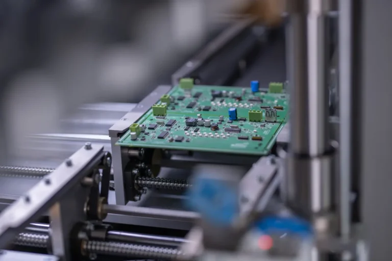
Boundary Scan Technology applied on EIIT – a Controlar company
The Synergy of Flash Programming and Boundary Scan in EIIT - a Controlar company Systems
EIIT integrates Flash Programming and Boundary Scan into our PCB test systems to provide our clients with precise, efficient, and industry-adapted solutions.
Benefits of This Integration in Our Test Systems
Conclusion
Flash Programming and Boundary Scan are essential technologies in the lifecycle of electronic devices, from prototype validation to production and maintenance. As electronics continue to evolve with increasingly complex and compact designs, the combination of these technologies becomes even more critical to ensure efficient production, precise testing, and robust maintenance.


